WAFER MARKER

Contribution for improving traceability of semiconductor manufacturing process
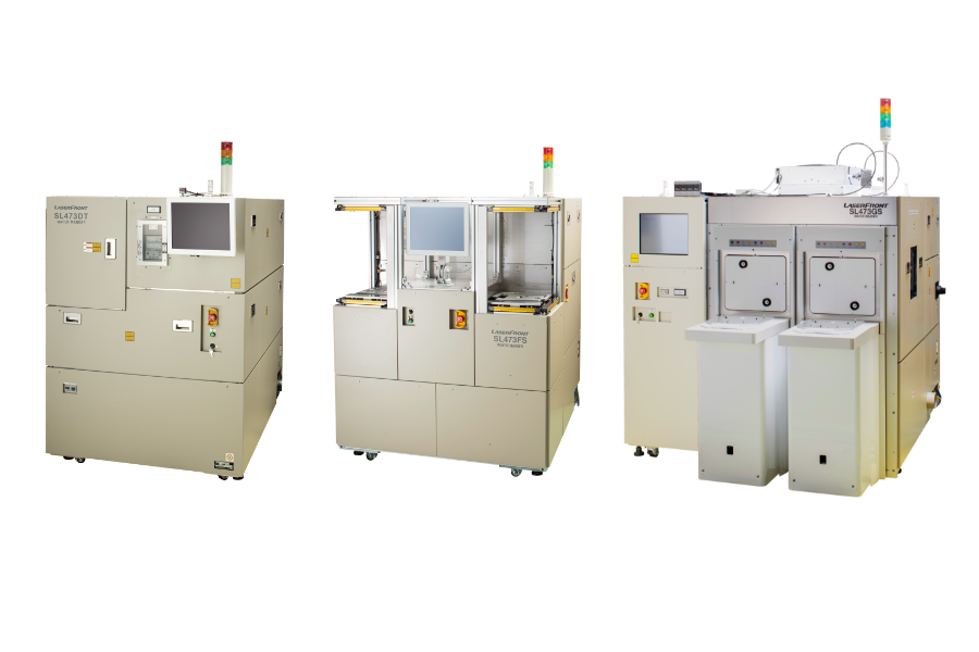
Wafer Marker SL473 Series
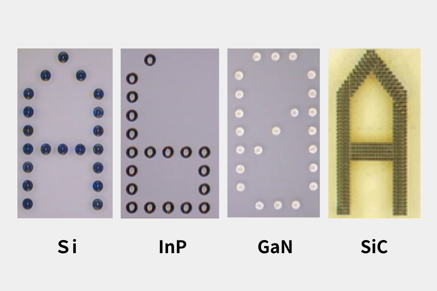
Wide products lineup not only for the marking on Si, GaAs wafer, but also for SiC, GaN, other wafer. Contribution for improving traceability of semiconductor manufacturing process with wide products line up for various wafer material, size, and production capacity
FEATURE
Stable marking with good visibility
Stable marking with good visibility by suitable laser oscillator for target wafer materials and the automated laser-power compensation function
Easy operation with high versatility
Easy operation changing recipes for marking on various different wafer sizes and materials.
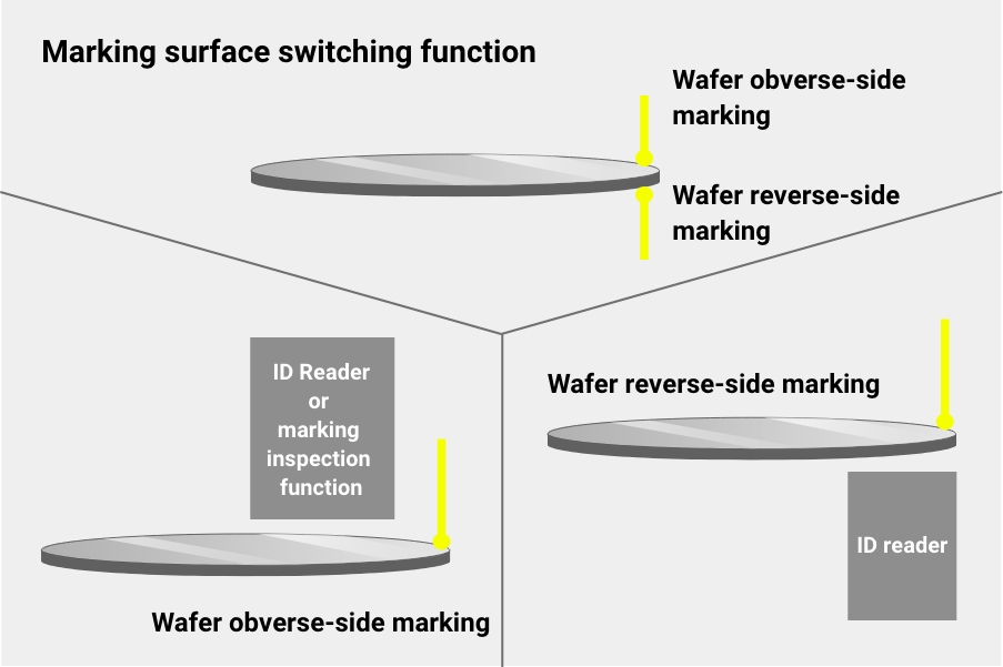
(Option: Multiple wafer size, reverse-side marking)
Extensive options and expandability
Online communication protocol, Wafer ID reader, Marking inspection function, Dust collector unit
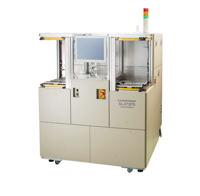
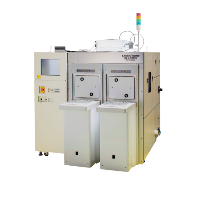
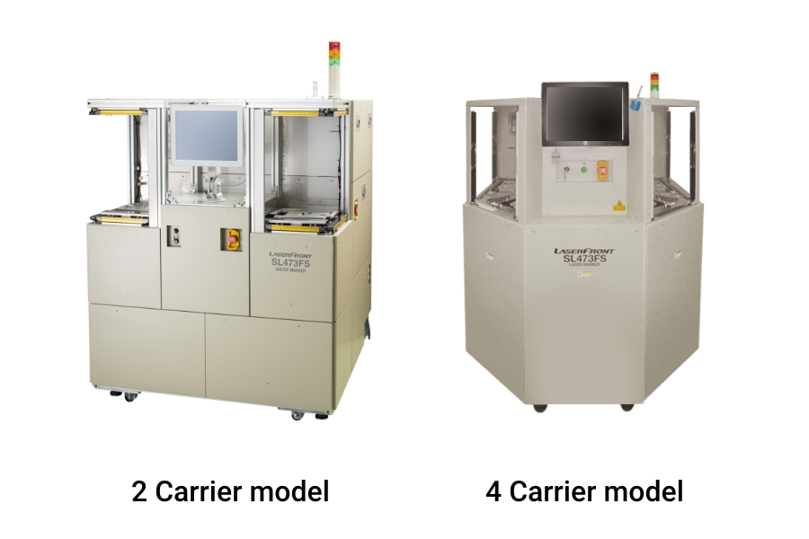
High-throughput Model
SL473FS / FT Series
Line up of two models: for 2-carrier and 4-carrier
APPLICATION
PURPOSE
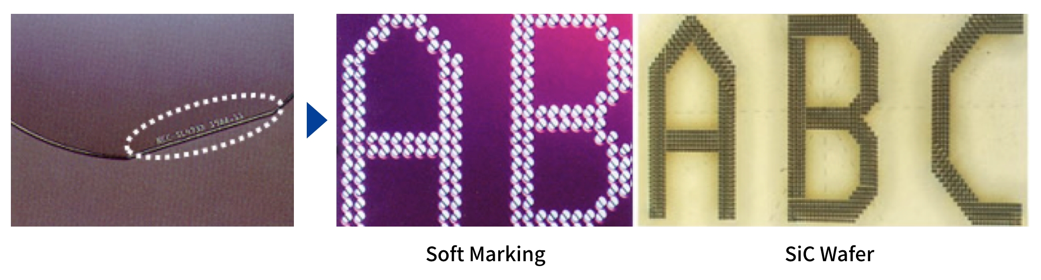
SL473FS Series: Soft marking for Si wafer, GaAs and InP wafer
SL473FT Series: SiC, GaN wafer and above mentioned wafer
MAIN SPECIFICATION
| Model | SL473FS Series | SL473FT Series |
|---|---|---|
| Laser Type | Nd: YAG-SHG laser Wavelength: 532 nm |
Nd: YLF-THG laser Wavelength: 349 nm |
| Number of port for Carrier | 2 or 4 | |
| Wafer Size | 4, 5, 6, 8 Inch each (Option: Multiple size) |
|
| Dimensions [mm] (*1) | Approx. 1,220 (W) x 1,244 (D) x 1,492 (H) ㎜ (2 carrier model) Approx. 1,220 (W) x 1,646 (D) x 1,492 (H) ㎜ (4 carrier model) |
|
| Weight(Main body) | 850 kg (2 carrier model) 900 kg (4 carrier model) |
|
- (*1) It does not include protrusions